If you’re selecting a polishing pad for semiconductor CMP, optical glass finishing, sapphire wafer processing, or industrial lapping, the choice between a polyurethane (PU) pad and a diamond lapping pad — and getting the hardness, material, and grit right — determines your surface quality, removal rate, and cost per part. This guide breaks down every factor you need to consider.
The first decision in how to choose a polishing pad is understanding the two primary categories. They serve fundamentally different roles in the polishing chain.
Polyurethane (PU) Pads
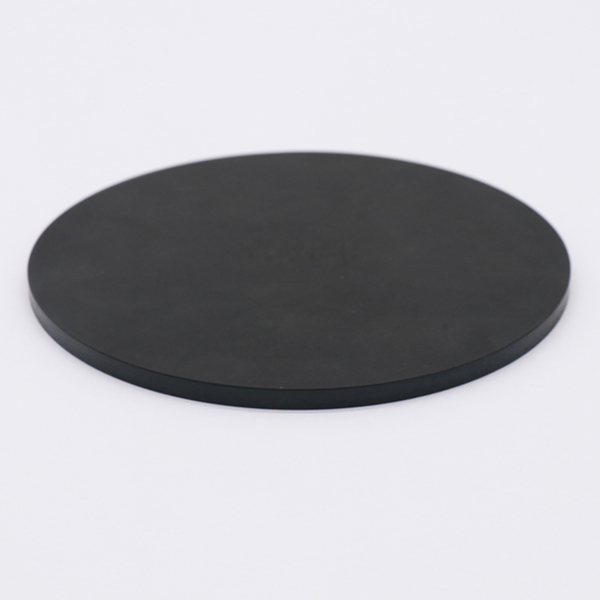
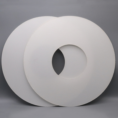
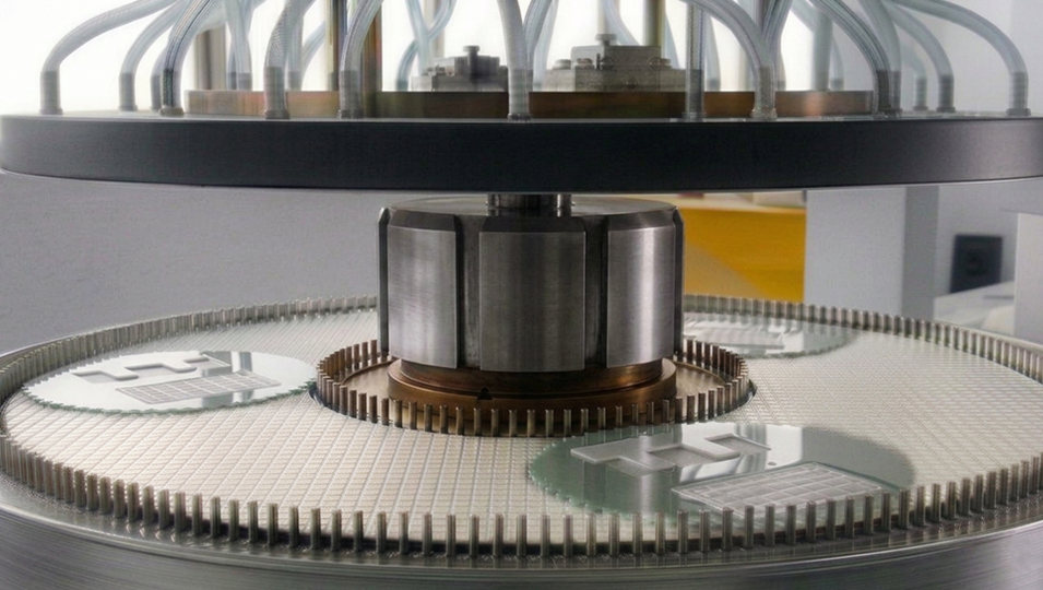
PU pads are cast from polyurethane foam, typically with a closed-pore microstructure created by incorporating hollow microspheres (such as PMMA) into the polymer matrix. These pores reduce the effective modulus of the pad surface, improve surface contact uniformity, and — as the pad is conditioned — continuously expose fresh pore structure to maintain slurry transport capability.
PU pads are used with a separate slurry containing abrasive particles (alumina, silica, ceria). The pad’s job is to transport slurry, distribute pressure, and carry away reaction byproducts. They dominate semiconductor CMP and are also used for optical glass, sapphire, and ceramics.
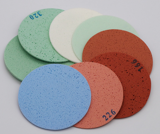
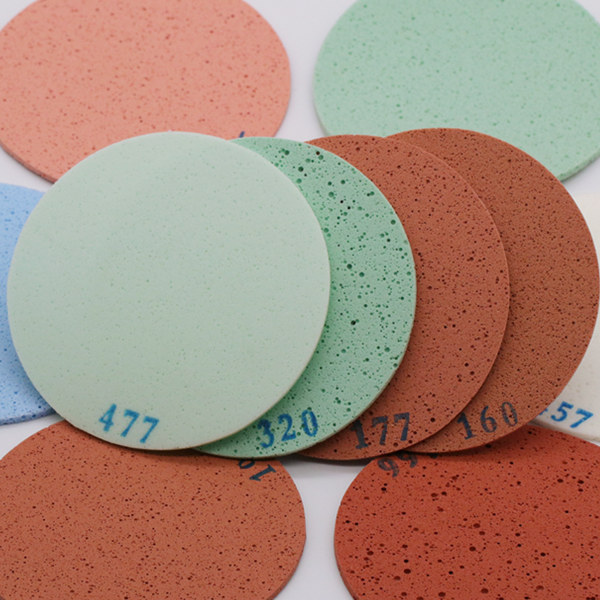
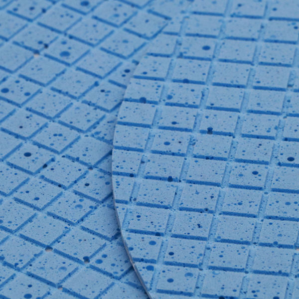
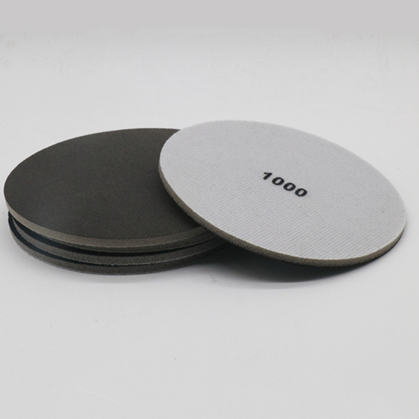
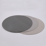
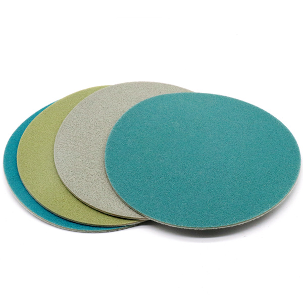
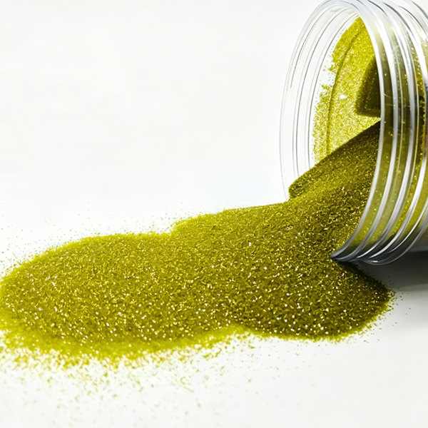
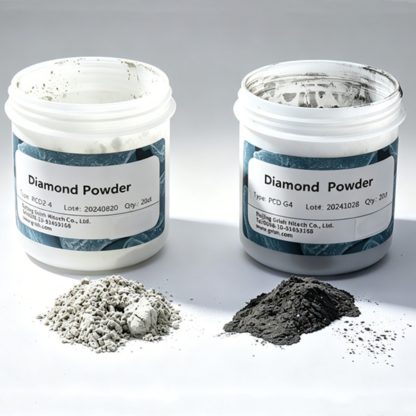
Diamond lapping pads belong to the category of fixed abrasive lapping technology. Unlike PU pads that rely on separate slurry, diamond lapping pads are constructed from diamond micro-powder compounded with resin into a uniquely designed pad structure, where the abrasive is fixed throughout the pad matrix rather than merely coated on the surface. This fixed-abrasive design means no free abrasive slurry is needed — only water or coolant — making the process more environmentally friendly and cost-effective.
Diamond lapping pads are available in particle sizes of 50 μm, 30 μm, 20 μm, 9 μm, and 4 μm, supporting a typical process sequence of: diamond disc coarse grinding → diamond disc medium grinding → thinning pad ultra-fine grinding → polishing pad finishing. They are widely used on glass substrates (microcrystalline, quartz, borosilicate, sapphire), semiconductor wafers (monocrystalline silicon, SiC), piezoelectric materials (lithium tantalate), and precision ceramics (alumina, aluminum nitride, silicon nitride).
Key Advantages of Fixed Abrasive Diamond Lapping Pads
- High selectivity: High selectivity for the processing zone with no material selectivity — achieves global planarization with less material removal
- Built-in elasticity: The resin-bonded structure provides controlled yield under grinding pressure, delivering better surface quality than loose-abrasive processes at the same grit size
- Long service life: Abrasive particles are fixed in the pad, resulting in higher utilization and longer pad life — reducing cost and waste
- Restorable performance: When the abrasive layer becomes dull, dressing (conditioning) restores sharpness and maintains consistent material removal rate
- Easy cleaning: Workpieces are easy to clean after processing, ensuring surface quality is maintained
- Environmentally friendly: No free abrasive slurry required — only water, reducing consumable costs
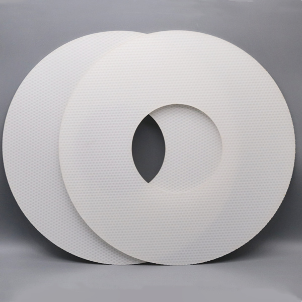
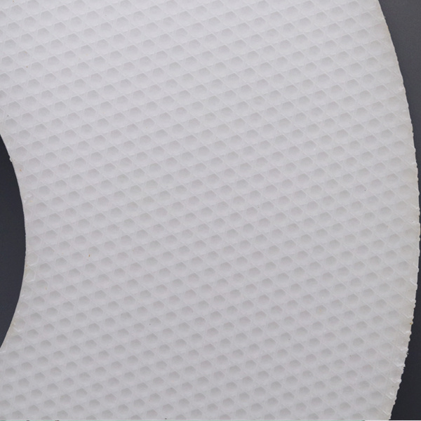
Polishing Pad Material Selection: What Determines What You Can Achieve
Polishing Pad Material Selection: The Foundation of CMP Performance
Polishing pad material selection is one of the most critical design decisions in CMP processes. It determines the pad’s hardness range, slurry retention capability, chemical compatibility, and thermal stability. Other design factors — such as groove design, pore structure, backing layer, and thickness — are optimized within the performance boundaries established by the base material.
Material-Determined vs Design-Determined Properties
Some polishing pad properties are primarily determined by the material itself, while others can be adjusted through pad design and manufacturing processes.
Material-determined properties include bulk hardness range, glass transition temperature (Tg), chemical resistance, and inherent pore structure. Design-determined properties, which can be optimized within the material’s limitations, include specific hardness values, pore size distribution, groove patterns, and pad thickness.
This distinction explains why different pad materials have fundamentally different performance capabilities. For example, a conventional polyurethane pad, regardless of formulation optimization, cannot achieve the same hardness and rigidity as a fixed-abrasive diamond polishing pad.
For polyurethane polishing pads, the glass transition temperature (Tg) typically ranges from 80–120°C, defining the thermal operating limit during polishing. By adjusting formulation parameters such as isocyanate concentration, polyol selection, and filler content, polyurethane pads can be engineered across a wide hardness range, typically from Shore D 30 to Shore D 70.

Polishing Pad Hardness: The Most Critical Selection Parameter
When selecting a CMP polishing pad, hardness is one of the most important factors influencing planarization performance, defect control, and surface quality. It represents the fundamental balance between material removal efficiency and surface defect risk.
Hard Polishing Pads (Shore D 55–65)
Hard pads have a higher elastic modulus, providing greater mechanical support during CMP. When the pad contacts a wafer surface with uneven topography, the rigid structure tends to bridge over recessed areas and concentrate pressure on elevated features.
This selective contact increases material removal from high points, allowing faster step-height reduction and improved global planarization.
Advantages:
- High planarization efficiency
- Excellent step-height reduction capability
- Improved within-wafer uniformity on patterned structures
Limitations:
- Higher contact stress at surface asperities
- Increased risk of scratches and defect generation
Typical applications:
- Oxide ILD CMP
- STI (Shallow Trench Isolation) CMP
- Tungsten plug CMP
Soft Polishing Pads (Shore A 28–50)
Soft pads have lower stiffness and better surface conformity. Under polishing pressure, they deform to follow wafer surface variations, allowing more uniform contact across both raised and recessed areas.
This improves surface finish and reduces defect risks, but the reduced mechanical support may limit planarization capability.
Advantages:
- Better surface finish
- Lower scratch generation
- Improved slurry distribution and retention
Limitations:
- Lower step-height reduction efficiency
- Higher risk of dishing on wide patterns
Typical applications:
- Copper buff polishing
- Final polishing steps
- Surface finishing processes
The Core Trade-Off: Planarization vs Surface Quality
A harder polishing pad provides stronger mechanical support and higher planarization efficiency, but excessive hardness can increase surface stress and defect formation. A softer pad improves conformity and surface quality but may sacrifice material removal efficiency.
Because of this inherent trade-off, many advanced CMP processes use a multi-step polishing strategy:
- Primary polishing stage: Hard pad for efficient planarization and topography correction
- Secondary polishing stage: Soft pad for surface refinement and defect reduction
Selecting the right polishing pad hardness requires balancing removal rate, planarization performance, scratch control, and final surface requirements based on the specific wafer material and CMP process.

CMP Pad Selection: Semiconductor-Specific Considerations
CMP pad selection follows a more rigorous framework than general polishing because semiconductor manufacturing demands nanometer-level precision. At 7nm nodes and below, a single chip undergoes 10-15 CMP steps, and each step may require a different pad.
| CMP Step |
Recommended Pad |
Hardness |
Why |
| Oxide ILD |
Hard PU pad (IC1000-type) |
Shore D 55-65 |
Maximum planarization efficiency |
| STI (Shallow Trench Isolation) |
Hard PU pad |
Shore D 55-65 |
Step-height reduction critical |
| Tungsten Plug |
Hard PU pad |
Shore D 55-65 |
High removal rate selectivity |
| Cu BEOL (primary) |
Hard PU pad |
Shore D 55-65 |
Planarization of Cu overburden |
| Cu Buff/Finish |
Soft PU or damping cloth |
Shore A 30-50 |
Low defect, remove residual Cu |
| Final Cleaning |
Soft pad / damping cloth |
Shore A 30-50 |
Surface finish, defect reduction |
| SiC / GaN (3rd gen semi) |
Special PU formulation |
Tuned for high hardness materials |
Balances hardness and flexibility |

Diamond Lapping Pad Selection: Particle Size, Structure, and Application
For hard, brittle materials that PU pads cannot efficiently process — sapphire, silicon carbide, quartz glass, precision ceramics — a diamond lapping pad using fixed abrasive technology is the right choice. Here’s how to select one.
1. Match Particle Size to Your Process Stage
Diamond lapping pads follow a progressive particle size sequence. The recommended workflow moves through four stages: start with a diamond disc for coarse grinding, switch to a finer diamond disc for medium grinding, transition to a thinning pad for ultra-fine grinding, and finish with a polishing pad. Larger particles remove material faster but leave a rougher surface; finer particles produce smooth finishes but remove slowly.
| Particle Size |
Stage |
Typical Application |
| 50 μm |
Coarse grinding / thinning |
Rapid stock removal on sapphire, ceramics, glass |
| 30 μm |
Medium grinding |
Dimensional accuracy, flattening |
| 20 μm |
Fine lapping |
Pre-polishing surface preparation |
| 9 μm |
Ultra-fine grinding |
Smooth finish before final polish |
| 4 μm |
Pre-polishing |
Mirror-quality surface preparation |
2. Material Removal Rate by Particle Size and Workpiece
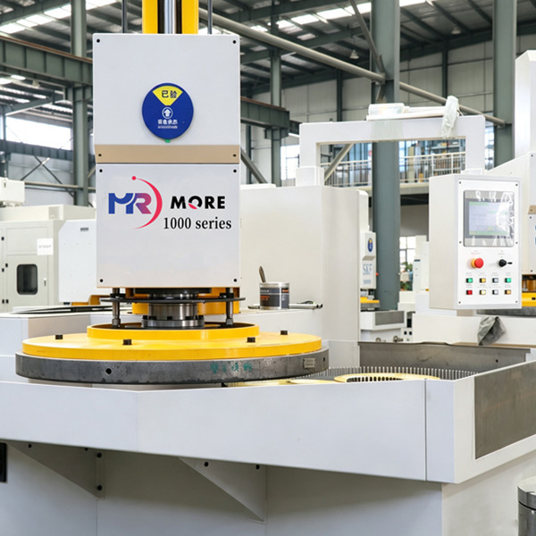
The interaction between particle size and workpiece material has a dramatic effect on removal rate. The table below presents laboratory measurements taken on a double-side lapping machine (9B model, 640 mm outer / 235 mm inner diameter) running at 238 kg down-force, 40 RPM, with 15 ml/min grinding aid and 30 ml/min coolant flow:
| Pad Type |
Sapphire (C-dir) |
ZrO₂ Ceramic |
Al₂O₃ Ceramic |
AlN Ceramic |
Glass |
SiO₂ / Si |
| 50 μm |
40 |
10 |
45 |
30 |
150 |
3 |
| 30 μm |
20 |
5 |
30 |
20 |
80 |
– |
| 20 μm |
15 |
2 |
20 |
15 |
50 |
– |
| 9 μm |
10 |
– |
– |
– |
30 |
– |
| 4 μm |
5 |
– |
– |
– |
20 |
– |
Finding the Best Polishing Pad: Key Takeaways
The best polishing pad for your application is the one that matches your material, process stage, and performance targets as a complete system. The right selection should balance material removal rate, surface quality, defect control, and process stability.
For semiconductor CMP:
Choose PU polishing pad hardness based on the trade-off between planarization efficiency and surface finish. Hard pads are preferred for initial planarization steps where topography removal is critical, while soft pads are better suited for finishing processes that require lower defect levels and improved surface quality.
For hard materials (sapphire, SiC, ceramics):
Fixed abrasive diamond lapping pads with progressive particle sizes from coarse to fine (such as 50 μm down to 4 μm) provide efficient material removal while gradually improving surface finish before final polishing.
For optical glass and precision optics:
PU polishing pads combined with ceria or alumina slurry are commonly selected. Pad hardness should be optimized according to the glass material and surface requirements, typically within the range of 75–90 Shore A.
Always plan pad conditioning:
Regular conditioning is essential to maintain stable polishing performance. Without proper conditioning, pad surface texture can degrade, reducing material removal efficiency and shortening pad service life.
Consider stacked pad structures:
When a single polishing pad cannot achieve both high planarization efficiency and excellent surface uniformity, a stacked structure combining a hard top pad with a softer sub-pad can provide a better balance between removal performance, stress distribution, and wafer uniformity.

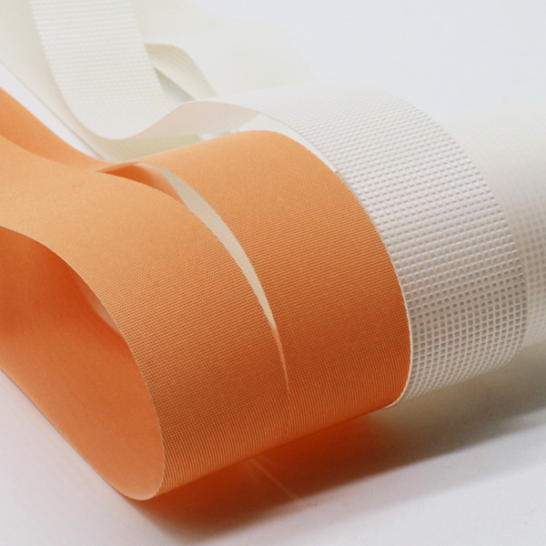 3D Structured Film (Cleaning belt for LCD panels)Flocked Pile Polishing Film for Roller Finishing and LCD Wiping
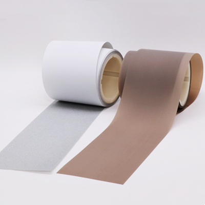 Polishing tape for repair defects and flatten protrusion points in LCD color filter process
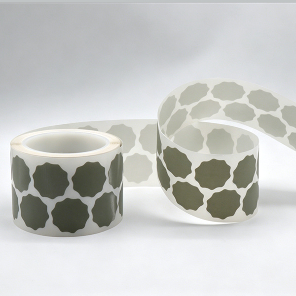 PSA Film Disc Roll for Fine Sanding and Finish of Automotive Coatings
 Electrostatic Coated Microfinishing Film Roll for Ultra-Fine Surface Finishing
 Precision Coated Diamond Roll for Fiber Optic & Microfinishing