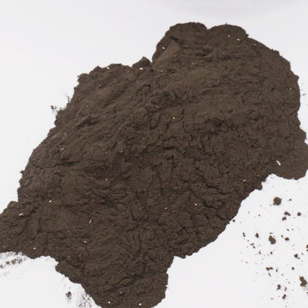
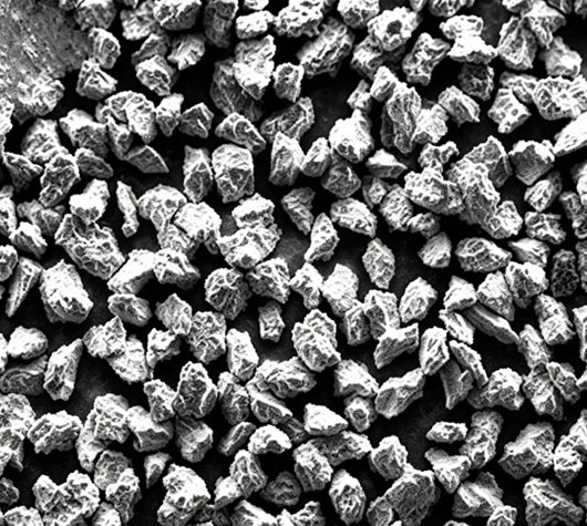
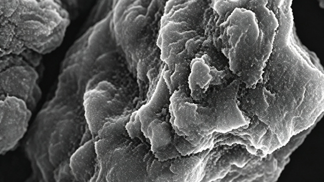
Typical Applications
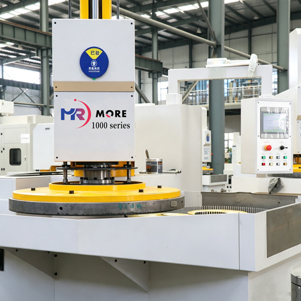
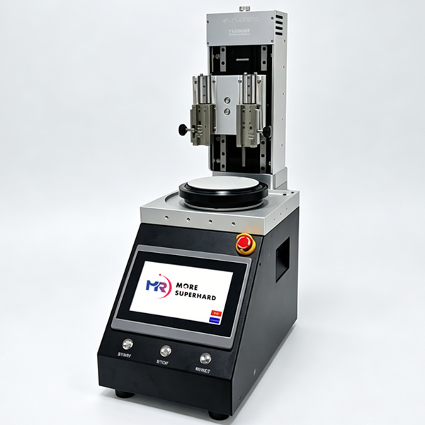
Optoelectronics: Polishing sapphire wafers, silicon wafers, GaN substrates, and ceramic components.
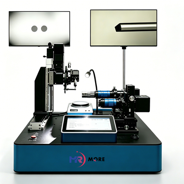
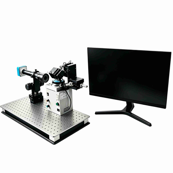
Precision Optics & Fiber: Processing fiber optic connectors, laser rods, and optical windows requiring high light transmittance.
Advanced Manufacturing: Machining magnetic head materials, magnetoresistive (MR) films, sputtered films, Molecular Beam Epitaxy (MBE) substrates, ferrites, and printed circuit boards (PCBs).
Oversized Particles Cause Surface Scratches
In precision polishing applications, a small number of oversized particles may create scratches on optical components, semiconductor wafers or precision molds.
Solution: Controlled classification processes help reduce oversized particle content and improve particle size consistency.
Particle Agglomeration Affects Slurry Stability
Poorly dispersed particles may agglomerate during slurry preparation, affecting polishing uniformity.
Solution: Uniform particle characteristics support better dispersion when formulating diamond slurries and polishing compounds.
Conventional Abrasives Lose Cutting Efficiency
Some abrasive particles become dull during prolonged polishing, reducing material removal efficiency.
Solution: The multi-crystal structure of polycrystalline diamond continuously generates new cutting edges through micro-fracture, helping maintain effective cutting action.
Batch Variation Leads to Inconsistent Polishing Results
Differences in particle size distribution between batches may affect polishing performance and process repeatability.
Solution: Controlled manufacturing and grading processes contribute to consistent particle characteristics from batch to batch.

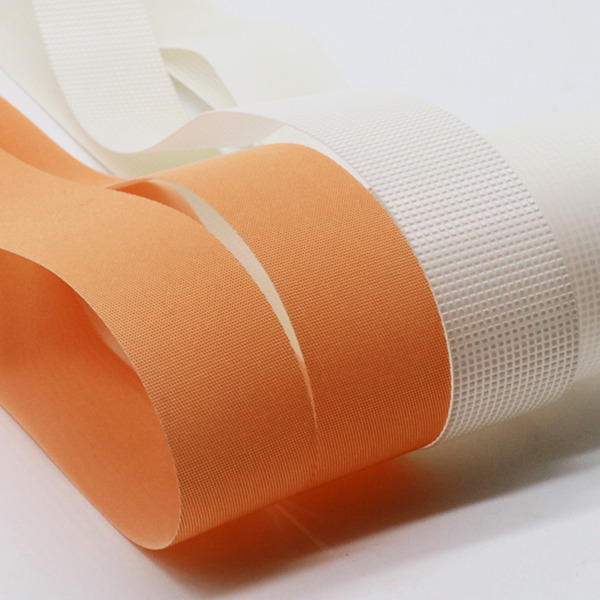 3D Structured Film (Cleaning belt for LCD panels)Flocked Pile Polishing Film for Roller Finishing and LCD Wiping
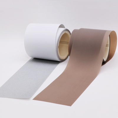 Polishing tape for repair defects and flatten protrusion points in LCD color filter process
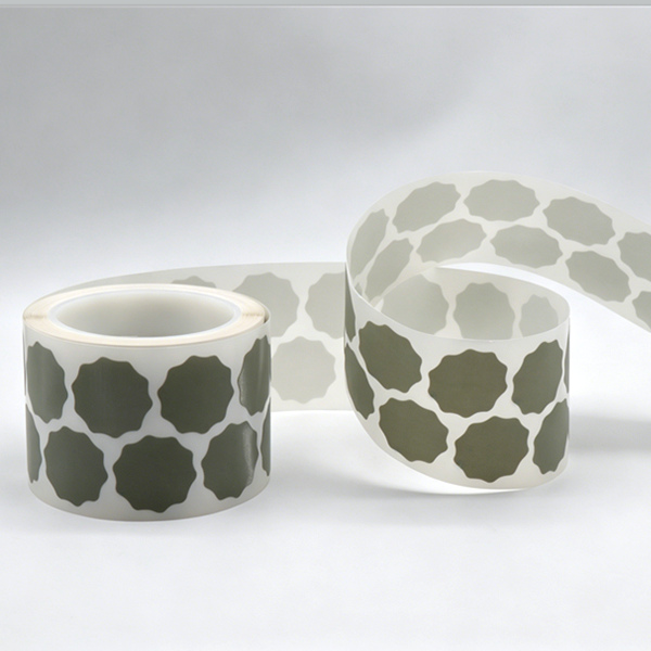 PSA Film Disc Roll for Fine Sanding and Finish of Automotive Coatings
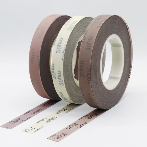 Electrostatic Coated Microfinishing Film Roll for Ultra-Fine Surface Finishing
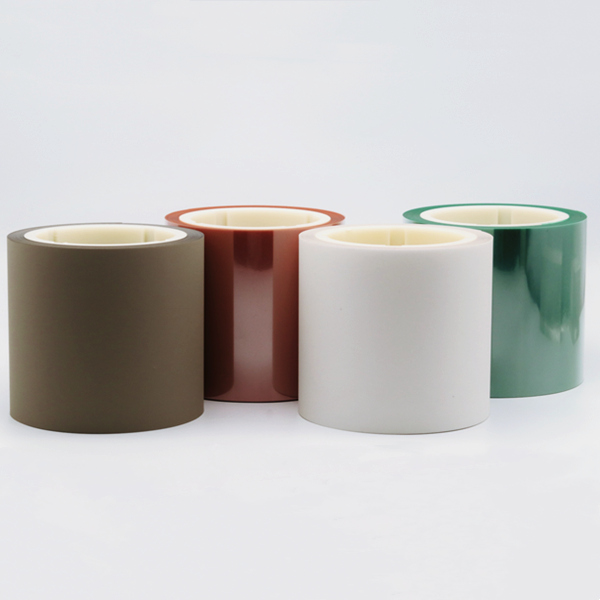 Precision Coated Diamond Roll for Fiber Optic & Microfinishing